CNC Machining for Different Industries
CNC machining technology is widely used in high-tech industries

CNC Machining for Semiconductors:
Precision Manufacturing at the Heart of the Chip Revolution
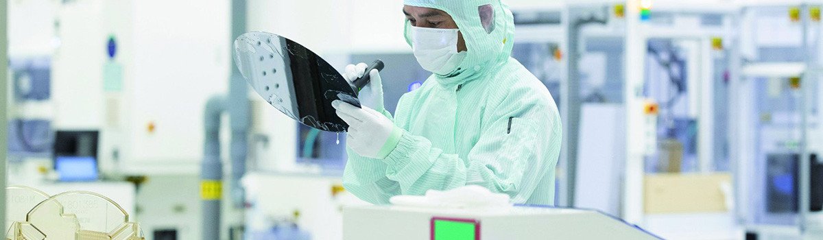
The semiconductor industry is the foundation of modern technology. From smartphones and laptops to artificial intelligence systems, electric vehicles, and advanced medical devices, almost nothing functions today without integrated circuits (ICs). At the core of this industry lies an uncompromising demand for precision measured in micrometres and even nanometres.
 
While photolithography, thin-film deposition, and etching dominate headlines when people talk about chip making, an often under-appreciated yet absolutely critical enabler exists behind the scenes: Computer Numerical Control (CNC) machining. High-precision CNC machining produces the ultra-flat, thermally stable, and geometrically perfect components that make semiconductor manufacturing equipment possible.
 
This article explores why CNC machining remains indispensable in the semiconductor ecosystem, which components rely on it, the materials and tolerances involved, the evolution of machine tools and processes, and the future challenges as the industry moves toward angstrom-era manufacturing.

Why CNC Machining Remains Essential in Semiconductor

EquipmentSemiconductor fabrication plants (fabs) contain hundreds of process tools, each costing anywhere from $10 million to over $400 million (in the case of ASML’s High-NA EUV systems). Almost every one of these tools contains hundreds or thousands of precision-machined parts.Key reasons CNC machining cannot be fully replaced:
  • Extreme geometric complexity: Many components have intricate internal cooling channels, high-aspect-ratio holes, thin walls, and complex 3D contours that are difficult or impossible to produce with casting, forging, or pure additive methods.
  • Material diversity: Semiconductor equipment uses aluminum, stainless steel (300-series, 316L, 17-4PH), titanium, copper, ceramics (Al₂O₃, AlN, SiC), invar, and superalloys. CNC can handle all of them.
  • Ultra-tight tolerances: Flatness of 1–5 µm across 450 mm diameters, hole position ±2 µm, surface roughness Ra < 0.1 µm, and parallelism < 2 µm are common.
  • Vacuum and plasma compatibility: Parts must survive aggressive fluorine or chlorine plasmas, ultra-high vacuum (10⁻⁹ mbar), and temperatures from −100 °C to >800 °C without outgassing or particle generation.
  • Repair and refurbishment: Many components (e.g., electrostatic chuck refurbishment) are repeatedly machined, recoated, and returned to service — a cycle only possible with subtractive processes.
In short, while the chip itself is made with optical and chemical processes, the machines that make the chip are overwhelmingly built with ultra-precision CNC machining.

Key Components Manufactured by CNC Machining

1. Vacuum Chambers and Large Structural Frames
Modern 300 mm and emerging 450 mm wafer tools contain aluminium or stainless-steel vacuum chambers that can weigh several tons yet must maintain wall parallelism and flange flatness to < 10 µm. These chambers are typically machined from 6061-T6 aluminium forgings or 316L stainless-steel plates on large 5-axis gantry mills with hydrostatic guideways.
2. Wafer Stages and Reticle Stages
The heart of EUV and DUV lithography tools is the wafer stage that moves 300 mm silicon wafers underneath the projection optics at accelerations > 8g while maintaining nanometre-level position accuracy. These stages are complex assemblies of ceramic (SiSiC, Zerodur, ULE glass) or aluminium parts machined to sub-micron tolerances and then hand-lapped or diamond-turned to final geometry.
3. Electrostatic Chucks (ESC)
Electrostatic chucks hold wafers perfectly flat during lithography, etching, and deposition. The dielectric surface (usually Al2O3 or AlN ceramic sprayed onto an aluminium or molybdenum base) must be machined and polished to peak-to-valley flatness < 1 µm across 300 mm. The base itself requires intricate internal cooling channels machined by high-speed CNC milling or wire EDM.
4. Gas Distribution Showerheads and Edge Rings
Plasma etch and deposition tools use showerheads with thousands of precisely sized and positioned holes (50–500 µm diameter) to deliver uniform process gases. These are typically machined from high-purity aluminium, silicon, or quartz, often using multi-axis CNC machining centres with ultrasonic or laser-assisted drilling capabilities.
5. Optical Components and Mounts
EUV lithography operates at 13.5 nm wavelength and uses reflective molybdenum-silicon multilayer mirrors. The mirror substrates (usually Zerodur or ULE glass) are first rough-machined by single-point diamond turning or precision grinding, then polished optically. The kinematic mounts that hold these mirrors must be CNC-machined from Invar or Super Invar to minimise thermal distortion.

Materials Used in Semiconductor CNC Machining

1. Aluminium Alloys
6061-T6 remains the workhorse due to excellent machinability, decent strength, and low cost. For higher stiffness and lower thermal expansion, proprietary aluminium alloys such as Al 6061-RAM2, RSA-6061, or Cearun™ (ceramic-reinforced aluminium) are used.
2. Low-Expansion Alloys
Invar 36 and Super Invar (with added cobalt) offer thermal expansion < 1 ppm/°C and are critical for reticle and wafer stage components.
3. Ceramics and Technical Glasses
  • Silicon-infiltrated silicon carbide (SiSiC)
  • Reaction-bonded silicon carbide (RBSC)
  • Zerodur® (Schott) and ULE® (Corning) ultra-low expansion glass
  • Aluminium nitride (AlN) and alumina (Al2O3) for electrostatic chucks

These brittle materials require specialised CNC processes: ultrasonic machining, ductile-regime grinding, or laser-assisted machining.

4. High-Purity Metals

Molybdenum, tungsten, and titanium are used for components exposed to fluorine plasmas. These refractory metals demand rigid, high-torque CNC machines and polycrystalline diamond (PCD) tooling.

Typical Semiconductor Components Made by CNC Machining

Component
Typical Material
Key Requirements
Tolerance Examples
Wafer chucks (ESC)
Alumina, AlN
Flatness < 3 µm, Ra < 0.05 µm, helium leak < 10⁻⁹
±2 µm hole position
Showerheads / Gas plates
Anodized Al, 316L SS
5000–20,000 holes Ø0.3–1.0 mm, ±5 µm position
< Ra 0.4 µm
Vacuum chamber walls
6061-T6, 5083 Al
Welded + machined, helium leak-tight
Flatness < 50 µm over 2 m
Electrode assemblies
OFHC copper, molybdenum
RF conductivity, cooling channels
±10 µm channel location
Lift pin assemblies
Ceramic-coated stainless
Wear resistance, particle control
Concentricity < 5 µm
Structural frames (EUV)
Invar 36, low-CTE alloys
Thermal stability < 50 ppb/K
Positional accuracy ±15 µm
Focus rings, edge rings
Silicon, quartz, SiC
Plasma erosion resistance
Profile tolerance ±10 µm
 
These parts range in size from a few millimeters to over 2 meters and in weight from grams to several tons.

Precision Levels and Metrology

Typical tolerances in semiconductor equipment machining:
Feature
Typical Tolerance
Measurement Method
Flatness (300 mm surface)
0.5–2 µm PV
Interferometry (Fizeau, Zygo)
Parallelism
1–5 µm
Electronic levels + interferometry
Hole position (thousands of holes)
±2–5 µm
Coordinate measuring machine (CMM)
Surface finish
Ra 0.025–0.1 µm
White-light interferometry
Cooling channel position
±10 µm
CT scanning or ultrasonic testing
 
Leading shops now routinely achieve “sub-micron” or even “100-nanometre” mechanical accuracy on components weighing hundreds of kilograms.

Evolution of CNC Machine Tools for Semiconductor Work

1. The 1990s–2000s Era
Large gantry mills (Waldrich Coburg, Parpas, FPT) with Heidenhain scales and glass-scale feedback dominated. Hydrostatic bearings and oil showers provided thermal stability.
2. The 2010s: Air-Bearing and Magnetic Levitation Stages
Companies such as Aerotech, Physik Instrumente (PI), and ALIO Industries introduced air-bearing linear motor stages with < 10 nm repeatability. These became the backbone of second-generation precision machining centres.
3. Current State (2020–2025)
  • Moore Nanotechnology and Precitech single-point diamond turning machines for EUV mirror substrates
  • Kern Microtechnik and Yasda micromachining centres achieving 100 nm form accuracy
  • DMG MORI ULTRASONIC series for ceramics
  • Fanuc ROBONANO α-NMiA: 0.1 nm programming resolution and 1 nm positioning resolution
  • Temperature-controlled shops held at ±0.01 °C with active vibration isolation foundations

Materials Challenges and Selection

1. Aluminum Alloys
6061-T6 and 5083 are workhorses due to excellent machinability and anodization response. Hard anodizing (Type III) creates a 25–50 µm Al₂O₃ layer that resists plasma attack. However, micropores in anodizing can trap particles — modern shops use multi-step sealing and proprietary coatings (e.g., Twin Wire Arc Spray Al₂O₃ or Y₂O₃ plasma spray).
2. Stainless Steels
316L is chosen for corrosion resistance against NF₃ and Cl₂ plasmas. Electropolishing to Ra < 0.2 µm is mandatory to reduce particle adhesion.
3. Ceramics
Alumina (99.8%), aluminum nitride, and silicon carbide are machined in the “green” state” using diamond tools, then sintered. Tolerances after sintering shrink 18–22%, requiring sophisticated shrinkage compensation models.
4. Low-CTE Alloys
Invar 36 and Super Invar are used in EUV and DUV lithography stages where nanometer stability is required across 10–40 °C temperature swings.
5. Refractory Metals
Molybdenum and tungsten are machined for high-temperature electrodes. These materials are extremely abrasive and require rigid machines with high-pressure coolant (70–100 bar).

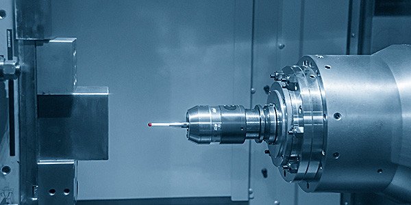
Critical Machining Processes

1. High-Speed Machining (HSM) of Aluminium

Spindle speeds 20,000–42,000 rpm, balanced PCD or single-crystal diamond tools, mist cooling, and look-ahead algorithms allow mirror-like finishes (Ra < 4 nm) in a single pass.

2. Ductile-Regime Machining of Ceramics

By keeping depth of cut below a critical threshold (typically < 1 µm), brittle materials can be machined in a ductile mode using ultra-sharp diamond tools, producing optical-quality surfaces without cracking.

3. Single-Point Diamond Turning (SPDT)
Essential for aspheric EUV mirror substrates. Machines operate in oil-mist or vacuum environments with sub-nanometre feedback.
6.4 Wire EDM and Sinker EDM
Used for deep cooling channels and intricate features in hardened materials. Modern generators achieve surface finishes < Ra 0.1 µm in a single skim cut.
5. Additive + Subtractive Hybrid Manufacturing
Emerging trend: 3D-print Invar or titanium near-net shapes, then finish-machine on the same platform (e.g., Hermle MPA or Lasertec DED hybrids).

Precision and Ultra-Precision CNC Requirements

Semiconductor parts routinely demand:
  • Positional accuracy: ±2–5 µm over 500–2000 mm travel
  • Repeatability: < 1 µm
  • Surface finish: Ra 0.025–0.1 µm on plasma-facing surfaces
  • Flatness: 1–3 µm over Ø300–450 mm
  • Parallelism/perpendicularity: < 3 µm
To achieve this, machine shops invest in:
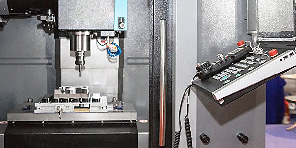
  • 5-axis or even 8-axis machining centers (e.g., Yasda, Makino, DMG MORI, Kern, Liechti)
  • Hydrostatic or air-bearing spindles running at 20,000–60,000 rpm
  • Thermal stabilization systems keeping machine temperature within ±0.1 °C
  • On-machine probing and laser tool setters with 0.1 µm resolution
  • Granite or polymer-concrete bases with active vibration isolation
Example: Yasda YBM-950V can achieve 1 µm volumetric accuracy over 900×500×400 mm thanks to a box-in-box structure and 0.05 µm resolution scales.

Lorem ipsum dolor sit amet, consectetur adipiscing elit. Ut elit tellus, luctus nec ullamcorper mattis, pulvinar dapibus leo.

Advanced Machining Techniques

1. High-Speed Machining (HSM) with Small Tools
Showerheads may have 15,000 holes of Ø0.5 mm drilled at 40,000 rpm with 0.1 mm micro end mills. Peck drilling with 100 bar through-tool coolant prevents chip re-welding.
2. Ultrasonic-Assisted Machining
For ceramics and quartz, 20–40 kHz ultrasonic vibration reduces cutting forces by 30–70%, dramatically improving surface finish and tool life.
3. Single-Point Diamond Turning (SPDT)
Used for infrared lenses and some copper electrodes. Surface finishes down to Ra 3–5 nm are routine.
4. 5-Axis Simultaneous Milling of Complex Geometries
Internal cooling channels with 1 mm diameter and 20:1 aspect ratio are machined using long-reach tapered tools and trochoidal toolpaths.
5. Hybrid Additive-Subtractive Processes
Some new components (e.g., conformal-cooled showerheads) are 3D printed in Inconel or copper via DMLS/LaserCusing, then finish-machined on the same machine to ±10 µm.

Metrology and Quality Assurance

Semiconductor parts undergo the most rigorous inspection in any industry:
  • Zeiss Prismo or Leitz PMM-C ultra-precision CMMs with ±0.3 µm uncertainty
  • Zygo GPI or 4D Technology phase-shifting interferometers for flatness
  • Bruker white-light interferometers for Ra < 50 nm surfaces
  • Helium mass-spectrometer leak testing to 10⁻¹⁰ mbar·L/s
  • Residual Gas Analysis (RGA) after 150 °C bake to confirm outgassing < 10⁻⁹ Torr·L/s/cm²
  • Particle counting via liquid particle counter (LPC) or laser particle scanner after ultrasonic cleaning
Many shops now use in-process metrology: Blum laser tool setters, Renishaw OMP400 strain-gauge probes, and Marposs acoustic emission sensors to detect micro-chipping in real time.

Cleanroom Machining and Post-Processing

Because particles >30 nm can kill a 3 nm transistor, many high-end shops have installed ISO 5 (Class 100) or ISO 4 cleanrooms directly around their precision machines.
 
Examples include:
  • Bullen Ultrasonics (USA)
  • Tyrolit CNC cleanroom facility (Austria)
  • Canon’s Utsunomiya precision machining cleanroom (Japan)
Post-machining cleaning sequences typically involve:
  1. High-pressure DI water + megasonic agitation
  2. Multi-step chemical cleaning (SC-1, SC-2, piranha)
  3. Ultra-pure N₂ blow-dry
  4. 150–200 °C vacuum bake
  5. Double-bagging in N₂-purged bags

Case Study: Machining an EUV Wafer Stage Baseplate

A typical 450 mm EUV wafer stage baseplate illustrates the complexity:
  • Material: SiSiC ceramic, 900 × 800 × 100 mm
  • Flatness requirement: < 1 µm PV across entire surface
  • 120 embedded cooling channels, 3 mm diameter, ±15 µm position
  • 600 threaded inserts (M4 helium-light)
  • Final surface: lapped to Ra < 50 nm
Process flow:
  1. Green machining of reaction-bonded blank
  2. Silicon infiltration and heat treatment
  3. Rough grinding on 5-axis machining centre
  4. Ductile-regime finish grinding with 1 µm depth of cut
  5. Magnetorheological finishing (MRF) for final form correction
  6. Metrology on Zygo VeriFire MST 600 mm aperture interferometer
  7. Final hand lapping if needed
Total machining time: 6–10 weeks per part. Cost: $800,000–$1.2 million.

Challenges as the Industry Moves to sub-2 nm Nodes

1. Angstrom-Level Stability
Future EUV high-NA tools will require stage positioning stability in the 50–100 picometre range. This pushes mechanical components toward fundamental material limits.
2. 450 mm Transition
Larger wafers demand even larger machined components with the same relative precision—an exponential increase in difficulty.
3. New Materials
Carbon-based materials (graphene coatings, diamond-like carbon), metal-matrix composites, and photonic structures will require entirely new machining paradigms.
4. Sustainability
The industry is under pressure to reduce energy, water, and chemical consumption. Machining shops are adopting minimum-quantity lubrication (MQL), cryogenic cooling, and recycling of aluminium chips.

Conclusion

While the spotlight in semiconductor news remains on lithography wavelength and transistor density, the reality is that no leading-edge chip can be manufactured without an army of ultra-precise mechanical components produced by CNC machining. From multi-ton vacuum chambers flat to a micron to ceramic wafer stages stable to a few atoms, CNC machining operates at the absolute frontier of what is mechanically possible.
 
As the industry races toward angstrom-scale features and 450 mm wafers, the demands on precision machining will only intensify. Shops that can deliver sub-micron accuracy on meter-scale parts, in exotic materials, under cleanroom conditions, will remain indispensable partners to ASML, Applied Materials, Lam Research, Tokyo Electron, and the chipmakers themselves.
 
In the end, the famous Moore’s Law is not just a story of physics and chemistry—it is also a triumph of mechanical engineering executed one perfectly machined component at a time.