CNC Machining for Electronics:
Precision Manufacturing in the Digital Age
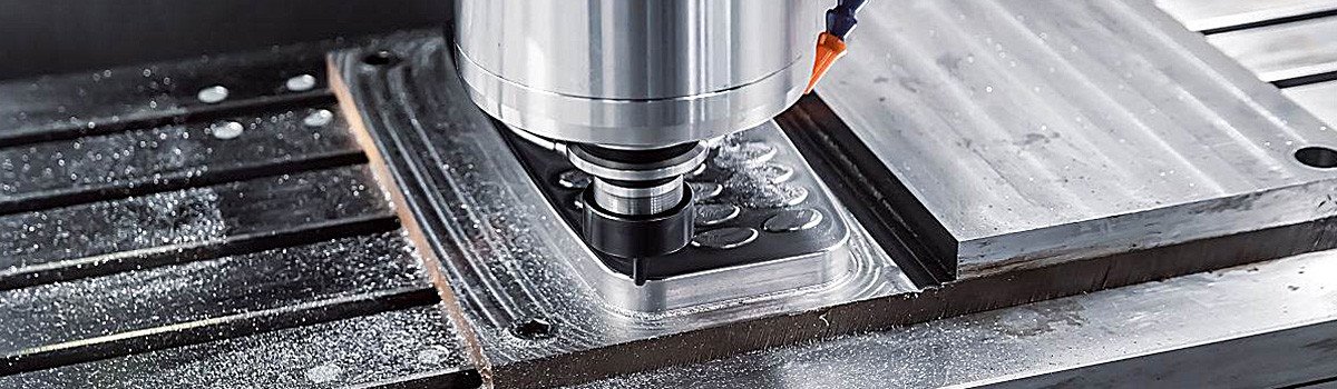
Table of Contents
ToggleWhy Electronics Manufacturers Still Choose CNC Machining
1. Unmatched Dimensional Accuracy and Tight Tolerances
- High-end metal 3D printing (DMLS, EBM): typical ±50–100 μm, with surface roughness often requiring extensive post-machining anyway
- Precision injection molding with metal inserts: ±20–50 μm at best, and highly dependent on mold quality and material shrinkage
- 5-axis CNC machining: ±2–5 μm routine, with premium shops achieving ±1 μm on stable setups
2. Extraordinary Material Versatility
- Oxygen-free copper (C10100/C10200): >398 W/m·K
- Tellurium copper (C14500): easier to machine while retaining ~95 % conductivity
- Tungsten-copper composites (WCu): for heat-spreaders that must match silicon CTE
- Aluminum 6061-T6 and 7075-T6 (aerospace-grade strength-to-weight)
- MIC-6 cast aluminum tooling plate (exceptionally stable for baseplates)
- Magnesium AZ31B/AZ61A (30 % lighter than aluminum with good EMI shielding)
- Aluminum nitride (AlN): ~170–220 W/m·K with near-zero electrical conductivity
- Machinable ceramics such as Macor and Shapal Hi-M Soft
- PEEK, Ultem 2300, Torlon 4203, PTFE—where metal simply cannot be used near sensitive RF circuitry
3. Complex Thermal Management Geometries That Other Processes Cannot Replicate
- Internal conformal cooling channels that follow the exact hotspot layout of a chip
- Pin-fin arrays with 0.2 mm diameters and aspect ratios >15:1
- Skived pure-copper fins 0.1–0.3 mm thick for maximum surface area
- Ultra-thin vapor chamber walls (<0.4 mm) with complex internal wick structures
4. The Sweet Spot: Prototyping Speed and Low-to-Medium Volume Economics
CNC with soft tooling, fixture automation, and sister tooling still beats the amortized cost of hard tooling required for die casting or MIM. Many programs never leave this volume range—especially in enterprise, defense, and high-reliability electronics.
Only at higher volumes do die casting, metal injection molding, or cold forging become attractive. Even then, secondary CNC operations are frequently required for datum surfaces, threads, tight-tolerance holes, and final cosmetic finishes.
5. Surface Finish, Hermeticity, and Reliability
Key Materials and Their Machining Characteristics
In precision electronics manufacturing, material selection and machinability directly determine whether a part meets thermal, electrical, mechanical, and reliability requirements. While hundreds of alloys and polymers exist, a small group dominates high-end enclosures, thermal management, RF components, and hermetic packages.
1. Aluminum Alloys – The Universal Baseline
- 6061-T6 and 6082: The default choice for housings, frames, and heat sinks. Excellent machinability (rated ~90–95% of free-machining brass), predictable anodizing response, and low cost. Takes mirror finishes with diamond-tipped or polished carbide tools.
- 7075-T651/T7351: Aerospace-grade strength (570 MPa UTS) at two-thirds the density of steel. Common in satellite electronics, military handheld devices, and high-end laptop chassis (e.g., MacBook unibody). Slightly gummy compared to 6061; requires sharp tools and rigid setups to prevent chatter on thin walls.
- MIC-6 and ATP-5 cast tooling plate: Precision-cast, stress-relieved plates with stability within 0.013 mm/m. The gold standard for optical benches, radar pallets, and large baseplates where flatness after machining is non-negotiable.
- Use 45–55° helix polished flutes with ZrN or AlTiN coating to eliminate built-up edge.
- Maintain balanced pressure on thin walls (<1.5 mm) using vacuum fixtures or low-melting alloy support.
- Leave 0.10–0.15 mm extra stock on surfaces receiving MIL-A-8625 Type III hard anodize (typically adds ~0.05–0.07 mm per side).
2. Copper and Copper Alloys – Thermal Champions
- C10100/C10200 Oxygen-Free (OFHC): >101% IACS electrical conductivity, >398 W/m·K thermal. Used in vapor chambers, high-power laser diode submounts, and AI accelerator cold plates.
- C11000 Electrolytic Tough Pitch (ETP): Slightly lower conductivity (~100% IACS) but cheaper and adequate for most heat spreaders.
- C14500 Tellurium Copper: The machinist’s best friend. Adding 0.5% tellurium breaks the chip and improves speeds/feeds by 3–4× over pure copper while retaining 90–95% IACS.
Copper is notoriously gummy. Long, stringy chips wrap around tools and wreck surface finish if not managed aggressively. Successful strategies include:
- Extremely sharp polycrystalline diamond (PCD) or positive-rake carbide inserts (0.05–0.1 mm hone).
- High-pressure through-tool coolant (70–100 bar) to break chips and cool the cutting zone.
- Exclusive climb milling and trochoidal toolpaths with ≤8–10% stepover in pockets deeper than 1× diameter.
- Constant chip-load monitoring; even slight variation causes work hardening and tool failure.
3. Magnesium Alloys – When Every Gram Counts
- AZ91D: Most common die-casting alloy; good corrosion resistance with proper coating.
- WE43 and Elektron 675: Rare-earth variants with superior strength and heat resistance up to 300 °C, used in aerospace electronics.
- Generous flood coolant or MQL with fire-suppression sensors.
- Explosion-proof chip vacuums and wet collectors.
- Toolpaths designed to produce short, broken chips rather than fines.
4. Specialty and Controlled-Expansion Alloys
- Kovar and Alloy 42: CTE matched to borosilicate glass for hermetic packages (TO headers, microwave feedthroughs). Require stress-relief cycles before and after machining to prevent warping during glass sealing.
- Invar 36: Near-zero CTE for stable optical mounts and satellite antenna bases.
- Molybdenum and Tungsten (pure or Cu-clad): High-temperature heat sinks in GaN radar T/R modules. Extremely abrasive; diamond tooling and low speeds (<50 m/min) are mandatory.
- Titanium Grade 5 (Ti-6Al-4V): Increasingly common in medical wearables and implantable devices that integrate electronics. Poor thermal conductivity demands rigid machines, sharp tools, and aggressive coolant.
Design for Manufacturability (DFM) in Electronics
1. Wall Thickness and Uniformity
2. Ribs and Bosses
Add ribs instead of thickening entire walls. Height ≤ 4× thickness to avoid sink marks and distortion.
3. Undercuts and Lifters
Avoid whenever possible. If unavoidable, use dovetail or dog-bone undercuts that can be machined with a lollipop cutter.
4. Threaded Holes
Specify roll-form (thread-forming) taps instead of cut taps when possible—stronger threads and no chips in blind holes.
5.Tolerances
Only tolerance what matters. A typical smartphone middle frame might have:
- ±0.02 mm on camera lens mounting surfaces
- ±0.05 mm on side walls
- ±0.10 mm on non-functional cosmetic areas
6. EMI Shielding Features
- Continuous knife-edge bosses for conductive gaskets
- Machined-in spring finger pockets
- Bosses for canned shield soldering
Key Applications of CNC Machining in Electronics
1. Enclosures and Structural Components
- Smartphone unibody frames (Apple iPhone 15 Pro – machined titanium)
- Laptop chassis (MacBook Air – 100% recycled aluminum CNC shells)
- Wearables (Apple Watch Series 10 – single-piece zirconium oxide + titanium)
2. Thermal Solutions
- Vapor chamber lids and bases (high-end gaming laptops, flagship smartphones)
- Liquid cold plates for AI servers (NVIDIA DGX systems)
- Skived copper heat sinks (telecom base stations)
- IGBT heat spreaders for electric vehicles
3. RF and Microwave Components
- Waveguide flanges and transitions (5G mmWave, satellite comms)
- Cavity filters and combiners
- Antenna feed horns machined from aluminum or plated brass
4. Connectors and Interposers
- High-speed board-to-board connectors (400+ Gbps)
- LGA/BGA sockets
- Test sockets for wafer-level and package-level testing
5. Optical Components
- Fiber-optic ferrules and alignment blocks
- Lens housings for LiDAR and ToF sensors
- Precision mirror mounts for AR/VR headsets
Materials Selection Guide for Electronic Applications
Copper Alloys
- C10100 / C10200 (OFHC) → Highest conductivity (401 W/m·K), used in vapor chambers
- C11000 (ETP) → Good balance of cost and performance
- C14500 (Tellurium Copper) → Free-machining, excellent for RF connectors
- C17510 (CuNi2Be) → High strength + moderate conductivity for spring contacts
Aluminum Alloys
- 6061-T6 → General purpose, excellent anodizing
- 7075-T6 → High strength-to-weight (aerospace electronics)
- MIC-6 → Cast jig plate with extreme stability for fixtures and baseplates
- AlSi10Mg → For metal 3D printing + CNC finishing hybrid parts
Magnesium
- AZ31B, AZ91D → Lightest structural metal, used in ultra-thin laptops and drones
- Requires specialized tooling and coolant strategies to avoid ignition risk
Plastics and Ceramics
- PEEK (Victrex 450G) → High temperature, low outgassing for satellite components
- Ultem 2300 (30% glass) → Flame retardant V-0, used in aircraft cabin electronics
- Aluminum Nitride (AlN) → 170–220 W/m·K + electrically insulating
- Macor → Machinable glass-ceramic for microwave tube insulators
Advanced CNC Techniques Used in Electronics
1. 5-Axis Simultaneous Machining
Enables undercuts, complex internal cooling channels, and single-setup production of vapor chamber lids. Typical cycle time reduction: 60–80% vs 3-axis + multiple setups.
2. Micro-Machining
- Tool diameters down to 0.05 mm
- Surface finishes Ra 0.1 μm or better
- Common for MEMS packages, medical hearing aids, and high-density connectors
3. Swiss-Type Turning
Dominant for circular connectors (M12, USB-C shells, circular MIL-spec). Can achieve:
- Concentricity < 3 μm
- Diameter tolerance ±2 μm
- Cycle times under 10 seconds for high-volume parts
4. Thin-Wall Machining
Smartphone frames often have walls 0.3–0.6 mm thick over 150 mm length. Requires:
- Vacuum fixtures or freeze-chucks
- Adaptive toolpaths with constant chip load
- High-pressure through-tool coolant
5. Hybrid Additive + CNC
- Print near-net-shape copper heat exchanger → CNC finish critical surfaces
- Reduces material waste from 80% to <20% in some vapor chamber designs
Surface Finishes and Post-Processing
1. Plating
- Electroless Nickel (EN) 5–15 μm → Corrosion protection + solderability
- Immersion Gold over EN → Wire bonding and high-frequency performance
- Hard Gold (Co-hardened) → Connector contacts
- Selective plating using CNC-machined masks
2. Anodizing
- Type II sulfuric → Cosmetic (consumer devices)
- Type III hardcoat 50 μm → Wear resistance (industrial, military)
3. Passivation and Iridite
- Aluminum passivation (MIL-DTL-81706)
- Chromate conversion (Alodine 1200) → Still used in aerospace despite RoHS concerns
4. Diamond-Like Carbon (DLC) and PVD
- For wear-resistant connector surfaces and sliding mechanisms
Design for Manufacturability (DFM) Guidelines Specific to Electronics
- Avoid deep pockets >10:1 depth-to-width in aluminum (vibration risk)
- Minimum wall thickness recommendations:
- Aluminum: 0.4 mm (smartphones), 0.8 mm (laptops)
- Magnesium: 0.5 mm
- Copper: 0.8 mm (thermal constraints)
- Specify corner radii ≥ 0.5 × wall thickness to reduce stress risers
- Draft angles: usually 0.5–1° per side for anodizing uniformity
- Tolerances: only tighten where absolutely needed (cost doubles for every halving of tolerance)
- Thermal relief slots around screw bosses to prevent warping during anodizing
Modern CNC Strategies for Electronics
1. 5-Axis Simultaneous Machining
Essential for complex liquid cold plates, waveguide assemblies, and curved smartphone frames. A single setup eliminates tolerance stack-up.
2. High-Speed Machining (HSM)
Spindle speeds 20,000–40,000 rpm, feed rates >20 m/min, and very light radial engagements (3–8%) produce mirror-like finishes on aluminum and copper while minimizing burring.
3. Adaptive Toolpaths (Vortex, Trochoidal, VoluMill)
These constant-engagement strategies reduce tool deflection and heat, allowing aggressive material removal rates in deep pockets without sacrificing thin-wall accuracy.
4. In-Process Probing and Adaptive Control
Renishaw probes measure critical features in-cycle and adjust offsets automatically—critical for long-running jobs where thermal growth can exceed tolerances.
5. Automation
Pallet pools, robotic load/unload, and sister tooling have brought CNC into medium-volume territory (10k–100k pcs/year) that used to belong exclusively to die casting.
Surface Finishing and Post-Processing
1. Anodizing (Type II and Type III)
2. Chemical Conversion (Alodine/Iridite)
3. Electroless Nickel
4. Diamond-Lapped and Polished Surfaces
5. Micro-Deburred Edges
Case Studies
1. Apple iPhone Unibody Frames
2. Nokia / Microsoft Liquid-Cooled Server Cold Plates (Project Olympus)
3. Tesla Battery Module Housings
Quality Control and Metrology in Electronics CNC
1. In-Process Monitoring
- Renishaw spindle probes
- Blum laser tool setters
- Marposs acoustic emission for micro-tool breakage detection
2. Final Inspection
- Zeiss Prismo CMM with ±0.5 μm accuracy
- Keyence LJ-X8000 inline 3D laser profilers
- Micro-Vu optical comparators for connector pin coplanarity (<10 μm)
3. Thermal Stability
Many shops maintain 20 ± 0.2 °C shop floor temperature for copper and Invar components.
Cost Drivers and Optimization Strategies
Major cost factors (in descending order):
- Material (copper and PEEK are expensive)
- Cycle time (5-axis simultaneous is slower)
- Tooling wear (diamond tools for ceramics, PCD for copper)
- Setup and programming
- Post-processing (plating, anodizing)
Optimization approaches:
- Family parts and tombstone fixturing
- Standardized raw material sizes
- Design parts for common tool diameters (0.5 mm, 1 mm, 2 mm, etc.)
- Use vacuum fixtures instead of custom soft jaws
Emerging Trends
1. Hybrid Additive-Subtractive Platforms
2. Blue-Laser Copper Welding + Machining
3. Digital Twin and Simulation-Driven Machining
VERICUT Force and Autodesk PowerMill adaptive modules predict and optimize cutting forces in real time, reducing thin-wall deflection to <5 μm.
4. Micro-Machining for 6G and Silicon Photonics
Kern Microtechnik and Fanuc Robodrill α-D21MiB5adv machines routinely drill 50 μm cooling holes and produce sub-10 μm alignment features for co-packaged optics.
5. Sustainability
Dry machining of aluminum with MQL, chip recycling, and re-melting of 6061 swarf back into extrusion billets have reduced carbon footprint by 40–60% in some European shops.